
Research
Core Innovation
High-Voltage Monolithic Active Pixel Sensors (HV-MAPS)
ADL’s HV-MAPS technology offers significant advantages for detector design, making it well-suited for various applications:
- Large-Area Scalability: Industrial-grade CMOS production enables sensors spanning 1 m² or more for space and collider experiments.
- Ultra-Fast Timing: Sub-nanosecond resolution for precision tracking in high-rate environments.
- Radiation Hardness: Robust performance in extreme conditions (e.g., LHC upgrades).
- Low-Mass Design: Ultra-thin sensors (50 µm) minimize scattering of particles and material interference.
Our Projects
Mu3e Experiment (PSI) – MuPix
First large-scale HV-MAPS pixel detector
We led the design and production of HV-MAPS for the pixel detector, delivering over 200 fabricated wafers.
AMEGO-X Space Telescope & Barrel Imaging Calorimeter of Electron Ion Collider – AstroPix
Gamma-ray detection in space and precise measurements of electron energy at Electron-Ion Collider (EIC).
DESY Test Beam Telescope – TelePix
A large-scale detector designed to enhance the performance of the DESY test beam telescope.
LHCb Tracker Upgrade – MightyPix
HV-MAPS have been proposed for the LHCb tracker upgrade. We design the sensor ASIC.
Medical Spinoff: Precision Cancer Therapy
We develop a novel MRI-compatible beam monitor for the Heidelberg Ion Beam Therapy Center.
Medical Spinoff: Ultrasound Computer Tomography (USCT)
Our medical spinoff project focuses an innovative imaging technology designed for early breast cancer detection.
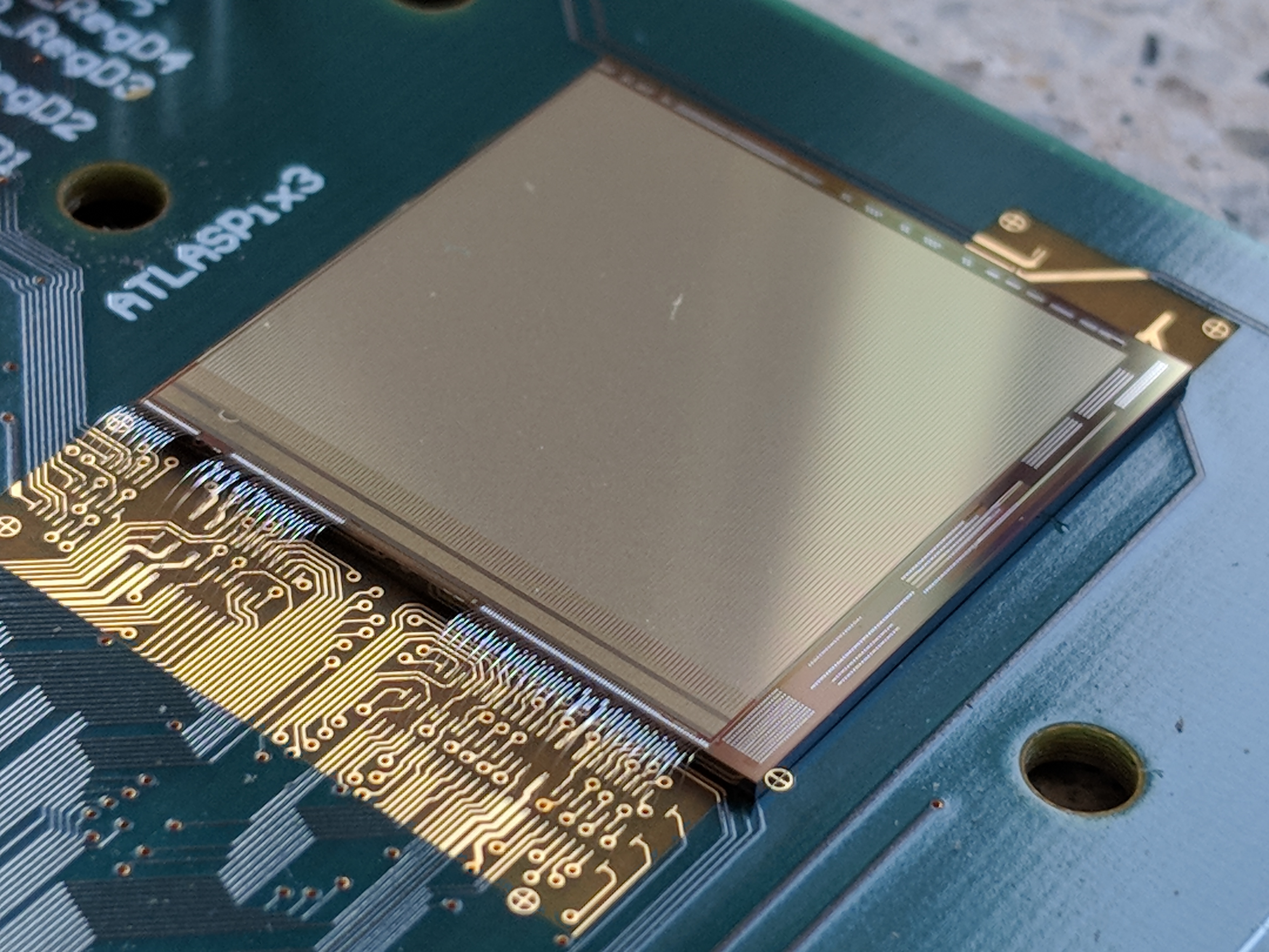
ATLASpix3: HV-MAPS demonstrator for research collaborations
A versatile HV-MAPS technology demonstrator created.
Hybrid Pixel Detectors
Pixel-readout chips designed for hybrid detectors, enabling advanced signal processing.
Advanced Sensor and Readout Technologies for High Time and Energy Resolutions
Pushing the limits of time and energy resolution with monolithic sensors and readout ASICs.
ASICs for Belle II pixel detector (KEK, Japan) - DCD and SWITCHER
We developed and delivered the radiation-tolerant ASICs for the Belle-II pixel detector.
ANDES Muon Detector (Argentina): Digital SiPM ASIC for single-photon detection
FASER (CERN): Ultra-fast ASIC design with the University of Geneva
Publication list from inspirehep.net
Selected publications
1. Large area HVCMOS sensor for particle physics ATLASPIX3:
journal homepage: https://ieeexplore.ieee.org/document/9373986
accepted manuscript: IEEE_JSSC_HVCMOS.pdf
Latest designs (user manuals)
1. TSI engineering run HVMAPS (HIT, LHCb, HVMAPS)
2. ATLASPIX3