
HV-MAPS
HVCMOS sensors or High Voltage Monolithic Active Pixel Sensors (HV-MAPS) represent a cutting-edge innovation in detector technology. These CMOS-based pixel sensors utilize high-voltage biasing to extend the active sensor volume, significantly enhancing performance metrics such as time resolution, detection efficiency and radiation tolerance. Designed for the precise detection of single ionizing particles, HVCMOS sensors are versatile tools with applications spanning high-energy physics, space exploration and medical imaging.
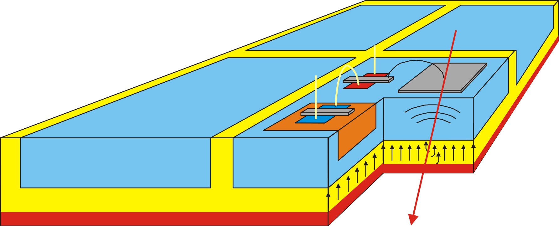
Key advantages of HV-MAPS are:
- Scalable industrial production processes that enables fabrication of large-area sensors
- High time resolution for precise tracking of particles
- Radiation hardness
- Ultra-thin sensor configurations that minimize material budget without compromising detection efficiency
The HV-MAPS architecture was first introduced and characterized in our publication: I. Peric, NIMA 582, no. 3, pp. 876-885, 2007
HV-MAPS R&D has been supported by German Federal Ministry of Education and Research (BMBF) and Helmholtz Programme Matter and Technology.